Logic Simulation of Circuits with Feedback
1. Tutorial Objectives
In this laboratory, you will gain experience in using LogicWorks(TM) to simulate latches, flip-flops, and some simple shift register circuits. In particular, you will:
* Simulate ring oscillators constructed from inverter chains.
* Simulate R-S and - latches constructed from cross coupled NOR gates and NAND gates respectively.
* Simulate a master/slave J-K flip-flop.
* Simulate positive and negative edge-triggered D flip-flops.
* Construct a two element shift register and determine the conditions under which the introduction of clock skew leads to incorrect results.
* Understand the limitations of the software simulator for simulating circuits with feedback, particularly for modeling race conditions, and how to establish initial conditions for the simulator.
Look back at Lab One if you need to review the use of LogicWorks(TM). It will be useful to remember how to use the Device Editor introduced there.
2. Getting Started: Ring Oscillators
Begin by invoking LogicWorks(TM), and create a schematic with three inverters in series. Feed the output of the last inverter stage back as an input to the first stage. Place probes at the outputs of the three inverter. What value do they read out?
The simulator must commence its operation making some assumptions about the initial values of all circuit nodes. LogicWorks(TM) understand the values logic 0, logic 1, undefined ( "X" ), as well as high impedance ( "Z" ). In the absence of other information, LogicWork assumes that all circuit nodes are undefined.
One way to initialize the simulation to a known state is to use the Clear Unknowns command under the Options menu. Do this now. What is the values displayed on the probes? Is this an inconsistent starting state for the simulation? If so, why?
While clearing the unknowns using the simulator command certainly has its uses, it is better to explicitly place the simulation in a known state. By the way, this is also a good idea in real hardware: at power up, a hardware system can (and as Mr. Murphy would said, will) come up in an unexpected or inconsistent state.
The simplest way to initialize the simulation is to specify starting waveforms in the timing window that are consistent. Do this by labeling the outputs of each inverter by the labels A, B, and C respectively. Place the simulation in single step mode. Then use the waveform tool to place an initial waveform on A, its complement on B, and B's complement on C. Now place the simulation in walking mode. What waveforms are displayed in the timing window?
Watch the values as they pass through the probes. If you see an "X" value that persists, you have not succeeded in correctly initializing the simulation. Place the simulation in single step mode and select Clear Timing under the Options menu. Try placing initial waveforms in the timing window once again (Note: an initial waveform on A with a transition in it should be sufficient to start up the simulation).
Single step the simulation if you are having difficulties following how the values change. It is not inconsistent in a running simulation to have the input and output of an inverter have the same value. Why is this?
What is the period of the output waveforms, i.e., how many time units are there between adjacent rising edges? What is the duty cycle of the waveforms, i.e., the percentage of time that the waveform is high versus low during its period? How wide, in time units, is the high time of the waveform?
It may be difficult to answer these questions because LogicWorks(TM) assumes unit delay, that is, each gate has a delay of one time unit. Go back and increase the gate delays to ten time units for each inverter. (Reminder: to do this, first select the gate, then select the Set Params command under the Options menu, and finally fill in 10 in the delay box.) Now what is the period, duty cycle, and high time of the waveforms?
Extend the circuit to five inverters in a chain. If you changed the delay of the inverters in the preceding paragraph, don't forget to follow the same process for the inverters you are now adding to the chain. You will probably need to reset the timing and re-initialize the simulation to get it into a consistent starting state. What do the waveforms look like now? What is the relationship between the number of gates in the chain and the shape of the waveform?
Under the Generic Devices submenu of the Libraries menu, you will discover a useful device called clock. Select this and place it on your schematic. Put a probe on its output and label it CLK. Select the device and then Select Params under the Options menu. LogicWorks(TM) allows you to set the high and low times of your clock. By default it has a period of 20 time units with a 50% duty cycle (i.e., high time of 10 time units, low time of 10 time units). Experiment with different settings and verify through simulation that the clock generates the waveform you specified.
3. R-S and Latches
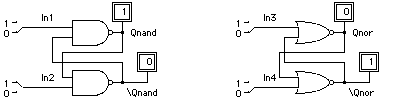
With LogicWorks(TM), draw two cross-coupled NAND gates and two cross coupled NOR gates. Places switches at the inputs and probes at the outputs. Call the outputs Qnand, , Qnor, and , and the inputs In1, In2, In3, and In4 (as shown in Figure 1)
.
Figure 1
What are the initial values read out on the probes? Do they include don't cares? If they do, place the latches in a consistent initial state. Now try all input combinations and write down your observations in a truth table format.
In terms of setting and resetting the outputs, what function is formed by driving In1 low? In2? In3 high? In4? Under what conditions are the outputs, supposedly complementary, driven to the same values? Circle these "forbidden" states "%20in%20your%20truth%20table.%20Under%20what%20conditions%20do%20the%20latches%20hold%20their" previous values?
It is not possible to observe the race condition inherent in latches implemented as above when using the input switches. Both inputs must change simultaneously to trigger the race. This can only happen when the inputs are specified through the timing window. Enter the waveforms as in Figure 2 and run the simulation. What do you see for the outputs?
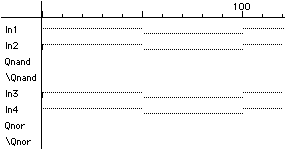
Figure 2
How does the race condition manifest itself in the output? What causes the race condition to terminate? Is it the same for both kinds of R-S latches?
For the rest of this laboratory, we will be using the R-S latch to build other kinds of building blocks. Create library modules for the R-S and - latches. Review how to do this from Tutorial One. To verify that you have done this correctly, build and simulate a transparent latch using the circuit diagram of Figure 3.
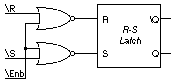
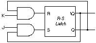
Figure 3
Verify that (1) reset and set only take place while the enable signal is asserted low, and (2) that reset and set are now active low. Jot down or print out the timing diagram that summarizes your observations.
4. J-K Master/Slave Flip-flop
First, construct a J-K flip-flop using the R-S latch building block as shown in Figure 4. Describe how this configuration avoids the "forbidden%20state" problem of the R-S latch. How would the schematic change if an - latch were used instead?
Since this is a circuit with feedback, its initial configuration may contain don't cares. Try the Clear Unknowns command. If the problem persists, you will need to force values on Q and , either by breaking the feedback and causing a set or reset, or by placing values on the nodes through the timing window.
Once the circuit is in a known state, fill in a truth table with inputs J, K, and Q (the current state) with Q+ as the next state output. Are there any cases under which Q and hold the same value? Draw or print the timing diagram that shows what happens to the outputs when J and K are both asserted. Explain the cause of this race condition.
Because the race condition still exists, this is not a good way to build the J-K flip-flop. Construct a master/slave J-K flip-flop as shown in Figure 5.

Figure 5
How would the schematic change if - latches had been used instead?
Perform the simulation using the timing diagram inputs of Figure 6. Sketch or print out the resulting waveform.
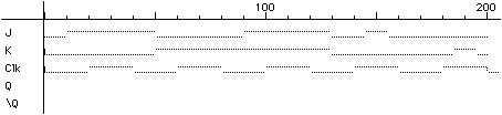
Figure 6
Under what conditions do you observe the 1's catching property of master/slave flip-flops? Explain why this takes place.
5. Edge-triggered Flip-flops
Ones catching in J-K flip-flops is a serious problem because it forces the combinational logic that generates J and K to be hazard-free. An alternative is to build an edge-triggered flip-flop. Enter the schematics for the two circuits of Figure 7.
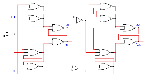
Figure 7
Use simulation to determine which circuit implements a positive edge-triggered D flip-flop and which implements a negative edge-triggered device. Sketch or print out your observed waveform that led you to your conclusion.
Revise the circuit by replacing the NOR gates with NAND gates. Do you still have an edge-triggered flip-flop? If so, which is positive edge-triggered and which is negative edge-triggered. Under the generic devices, LogicWorks(TM) lists a J-K flip-flop. Verify whether this device behaves like a master/slave flip-flop or an edge-triggered flip-flop. When do the outputs change? Does it exhibit ones catching? Be sure to wire the preset and preclear inputs to a logic one (or a switch: you can use the switch to get the outputs into a known state).
Also under this menu, you will find a generic D flip-flop. Use simulation to determine whether it is a positive or negative edge-triggered flip-flop.
6. Simple Shift Register and Clock Skew
Use the generic D flip-flop to construct a simple two-bit shift register as shown in Figure 8.
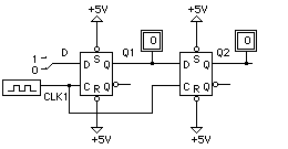
Figure 8
Demonstrate that the configuration implements a shift register by drawing the timing diagrams that verify that the first stage flip-flop successfully passes on its old output to the second stage flip-flop before this value changes.
Add some clock skew by placing two inverters between the clock and the clock input to the second stage flip-flop. What happens now? Draw the timing diagrams that indicate the incorrect behavior of the shift register.
LogicWorks(TM) does not model set-up and hold times, but the flip-flop does have a propagation delay that can be changed. Select the first stage flip-flop and then the Set Params item under the Options menu. Set the delay to 5 time units, and repeat the process for the second stage flip-flop. Repeat the steps you did in the previous paragraph. Does the shift register behave properly now? It should! Sketch the timing diagrams and explain why increasing the propagation delay led to correct operation.
7. Extra Credit Work (10 points)
Modify the schematic of the master/slave flip-flop to include an ability to asynchronously preset (force Q to one) or preclear (force Q to zero) the outputs. By asynchronous, we mean that the function takes place independently of the clock signal. Draw the schematic and verify its proper operation through simulation.
Modify the schematics of the edge-triggered D flip-flops to support an asynchronous preset and preclear. Verify through simulation that the operations work as expected.
8. Review
In this laboratory, we have used LogicWorks(TM) to simulate the operation of a number of simple but important circuits with feedback. We have examined the R-S latch, observed its forbidden state, and corrected this problem with the J-K flip-flop. However, the J-K flip-flop, when implemented as a master/slave device, suffers from "ones%20catching," a problem that forces the designer to avoid hazards in his/her circuits. This last problem was solved by introducing edge-triggered flip-flops.
Perhaps the most difficult problem in simulating circuits with feedback is getting them into a known initial state. With LogicWorks(TM) this is most easily accomplished by forcing values onto circuit nodes by using the timing window. It is not a bad idea to build the circuit with some self-starting logic, forcing them into a known state at power-up. For flip-flops, this can be achieved by including preset and preclear inputs. The generic devices supported by LogicWorks(TM) and most flip-flops in the TTL catalog have such inputs.
Once you have the confidence that you can use LogicWorks(TM) to simulate circuits with feedback, you should be able to use this tool for all your future laboratories and design projects.